Your trusted provider of Gas Abatement Systems
408-887-6132
BAZM Blog
The BAZM Blog
BOC Edwards TCS Gas Abatement System
July 18, 2022
This BOC Edwards TCS gas abatement system has arrived at our CA location. This system was originally owned by Intel. It is very clean, as it was used on a clean application, just ozone and NF3. It appears complete with the exception of the covers for the water recirculation unit (WRU). We have several Edwards WRU panels in stock and those panels should fit.
Read More
Airgard Cyclone Gas Abatement System
July 20, 2022
We have just taken receipt of an Airgard Cyclone gas abatement system. This is a very popular model of water scrubber given its simplicity and reliability. This particular system is like new on the outside, and it includes the explosion cage and entry cleaning mechanism. We do not expect this scrubber to be available for long so if interested please request a quote asap.
Read More
Used Cyclone Airgards
We have received two Airgards in "like new condition." They are identical and include the following options: pH control, explosion cabinet, entry cleaning mechanism. They are located in San Diego County and came from the Toshiba, California facility. Please call 619-346-0826 or email mike@bazmsolutions.com for a quote.
Read More
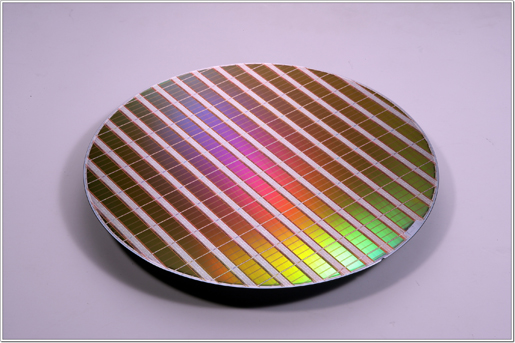
Oxide Etch Application Notes
The removal of thin films from the surface of a wafer is an important step in the manufacture of today's semiconductor devices. One of the most important removal steps is the patterning of silicon dioxide (often simply called oxide) layers which serve as transistor gates, and as insulation between layers of a microchip. The wafer is first patterned by photolithography, and then the etching process removes the exposed areas, transferring the pattern to the oxide layer.
Read More
Metal Etch Application Notes
The removal of thin films from the surface of a wafer is an important step in the manufacture of today’s semiconductor devices. One of the most important removal steps is the patterning of metal layers which serve as connections between layers on a microchip, or other semiconductor device. The wafer is first patterned by photolithography, and then the etching process removes exposed metal areas, transferring the pattern to the metal layer.
Read More
Ion Implantation
To accurately understand the abatement issues for any given process, it is necessary to understand the process in the tool, the chemicals that are put in, and how the process modifies them. The following overview represents our understanding of this process and is the basis of this recommendation.
Read More
Why Gas Scrubbing is Needed?
Greenhouse Abatement in the Semiconductor Industry
The manufacture of semiconductors requires the use of perfluorinated compounds (PFCs), namely C2F6, CF4, NF3, and SF6, which contribute to global warming. According to data from 2015, the semiconductor industry only accounts for about 0.18% of the total greenhouse emissions from US industrial sectors. Nevertheless, the semiconductor industry is taking steps to reduce its emissions to mitigate the effects of global warming.
Read More
12-17-18
It is the end of another year, and time to stock the shelves. Fortunately, here at BAZM we are already fully stocked with gas abatement systems and spare parts that are ready to ship from California. Avoid having your budget reduced for 2019, place your orders now for immediate shipment.
As always, if you have any technical questions, give us a call at 408-887-6132.
Brian Kingston
VP of Sales
July 18, 2022
This BOC Edwards TCS gas abatement system has arrived at our CA location. This system was originally owned by Intel. It is very clean, as it was used on a clean application, just ozone and NF3. It appears complete with the exception of the covers for the water recirculation unit (WRU). We have several Edwards WRU panels in stock and those panels should fit.
Read More
Airgard Cyclone Gas Abatement System
July 20, 2022
We have just taken receipt of an Airgard Cyclone gas abatement system. This is a very popular model of water scrubber given its simplicity and reliability. This particular system is like new on the outside, and it includes the explosion cage and entry cleaning mechanism. We do not expect this scrubber to be available for long so if interested please request a quote asap.
Read More
Used Cyclone Airgards
We have received two Airgards in "like new condition." They are identical and include the following options: pH control, explosion cabinet, entry cleaning mechanism. They are located in San Diego County and came from the Toshiba, California facility. Please call 619-346-0826 or email mike@bazmsolutions.com for a quote.
Read More
Oxide Etch Application Notes
The removal of thin films from the surface of a wafer is an important step in the manufacture of today's semiconductor devices. One of the most important removal steps is the patterning of silicon dioxide (often simply called oxide) layers which serve as transistor gates, and as insulation between layers of a microchip. The wafer is first patterned by photolithography, and then the etching process removes the exposed areas, transferring the pattern to the oxide layer.
Read More
Metal Etch Application Notes
The removal of thin films from the surface of a wafer is an important step in the manufacture of today’s semiconductor devices. One of the most important removal steps is the patterning of metal layers which serve as connections between layers on a microchip, or other semiconductor device. The wafer is first patterned by photolithography, and then the etching process removes exposed metal areas, transferring the pattern to the metal layer.
Read More
Ion Implantation
To accurately understand the abatement issues for any given process, it is necessary to understand the process in the tool, the chemicals that are put in, and how the process modifies them. The following overview represents our understanding of this process and is the basis of this recommendation.
Read More
Why Gas Scrubbing is Needed?
- Prevention of exhaust line clogging or corrosion.
- Eliminates transporting hazardous gases large distances.
- Regulatory requirements
Greenhouse Abatement in the Semiconductor Industry
The manufacture of semiconductors requires the use of perfluorinated compounds (PFCs), namely C2F6, CF4, NF3, and SF6, which contribute to global warming. According to data from 2015, the semiconductor industry only accounts for about 0.18% of the total greenhouse emissions from US industrial sectors. Nevertheless, the semiconductor industry is taking steps to reduce its emissions to mitigate the effects of global warming.
Read More
12-17-18
It is the end of another year, and time to stock the shelves. Fortunately, here at BAZM we are already fully stocked with gas abatement systems and spare parts that are ready to ship from California. Avoid having your budget reduced for 2019, place your orders now for immediate shipment.
As always, if you have any technical questions, give us a call at 408-887-6132.
Brian Kingston
VP of Sales
©Copyright BAZM Solutions